Carbon nanotubes have long been recognized as a promising material for the storage of hydrogen (read for background: "New carbon nanotube hydrogen storage results surpass Freedom Car requirements"). Back in 2003, researchers first synthesized carbon nanoscrolls – another carbon nanomaterial similar to multi-walled carbon nanotubes – that was reported to be promising for hydrogen storage

Graphene, multi-walled carbon nanotube, carbon nanoscroll
Carbon nanoscrolls (CNS) can be obtained by rolling up a graphene sheet into a tubular structure. In contrast to multi-walled carbon nanotubes (MWCNTs), with CNS one can vary the distance between layers, a property that might be crucial for gas storage applications. CNS are also expected to be useful in other nanotechnology applications, for instance in nanoelectronics, since they inherit some properties from both graphene and carbon nanotubes, e.g. high mechanical strength and carrier mobility. However, theoretical calculations also predict some unusual electronic and optical properties of CNS due to their unique topology.
"Although there are abundant theoretical predictions, few experimental investigations on CNS have been reported" says Kaili Jiang. "For instance, up to now its electronic structure remains experimentally untouched, either through optical methods or transport measurements. The challenges are how to fabricate high-purity and high-quality CNS and integrate them into devices."
Previously, several methods have been developed to make CNS. However, they were hard to control, difficult to purify, and the fabricated scrolls were found to possess poor morphology. Now, Jiang and his team at the Department of Physics and Tsinghua-Foxconn Nanotechnology Research Center at Tsinghua University in Beijing have developed a simple and effective technique for fabricating high-quality CNS. This work is based on the development of fabricating and characterizing single-layer graphene on substrate. It will be helpful for exploring both the physical properties and applications of CNS.
"During our fabrication of a graphene-based device using electron-beam-lithography, we found that some 2D graphene is likely to shrink to a 1D fiber-like structure when spinning the photoresist," Xu Xie tells Nanowerk. "At first we tried our best to avoid it because we actually had hoped to obtained 2D graphene devices. However, Professor Jiang thought the shrunk graphene might have interesting properties to explore, so we tried to fabricate it intentionally and then characterize it. Since we do not want to work with a photoresist (which is hard to clean and might affect the physical properties of graphene) we experimented with some chemical solutions. Finally we found that isopropyl alcohol (IPA) is a good candidate and it is the interaction between IPA solutions and the graphene surface that causes the graphene to roll up."
Xie, a graduate student in Jiang's group, together with Long Ju, is first author of a recent paper in Nano Letters that reports the team's findings (Controlled Fabrication of High-Quality Carbon Nanoscrolls from Monolayer Graphene). Xie and Ju outline the four steps they followed for fabricating the CNS:
1) First, graphene was extracted by mechanical exfoliation of natural graphite on a silicon wafer covered with 285 nm silicon dioxide and then immersed this chip with graphene into IPA solution. Now, the upper and lower surfaces of the graphene were in contact with IPA and silicon dioxide respectively, resulting in a surface strain in the graphene. This surface strain served as one of the driving forces to bend the graphene sheet.
2) Following the immersion into IPA solution, the edges of the graphene sheet were lifted up from the substrate by the surface strain. Then IPA molecules entered into the space between graphene and the substrate, which also facilitated the detachment of the graphene.
3) In the third step, the detached parts of the graphene curved due to perturbations in the solution environment. Once the free end touched another part of the graphene by chance, the π-π interaction of the overlapped parts decreased the total free energy of graphene, even though the curvature energy increased due to bending.
4) The scrolling process proceeded continuously in the final step, that is, the graphene became detached from the substrate and rolled up bit by bit until a scroll was formed with a decrease in total free energy.
"Based on this 4-step analysis, we optimized the scrolling process in three aspects" say Xu Xie and Long Ju. "Firstly, we found that pure IPA was too harsh for scrolling – if the graphene detaches from the substrate more quickly than it scrolls, direct folding might occur – but that we could affect the scrolling speed with different concentrations. Secondly, the shape of the graphene sheet is important; a long smooth edge was beneficial for scrolling and the sheets tended to scroll along this edge. And lastly, we noticed that the scrolling process is sensitive to contamination and that heavily contaminated graphene is difficult to roll. Therefore, in order to fabricate high-quality CNS, the graphene needs to be carefully protected"
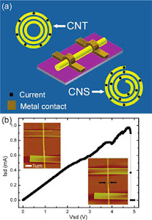
a) Schematic representations of current conduction at low bias. For CNT, only the outermost shell (which is in direct contact with the metal electrodes) sustains current. For CNS, the current extends to the whole scrolled graphene layer. (b) Current-voltage (I-V) curve measured under ambient conditions showing the high-bias electrical characteristics of a CNS about 50 nm in diameter. The breakdown point, which shows the diameter thinning after breakdown, lies midway between the two electrodes.
The researchers also conduct an interesting comparison of the current conduction characteristics of carbon nanoscrolls and multi-walled carbon nanotubes.
"For MWCNTs, only the outermost shell participates in conduction at low bias; the inner shells can only couple to the external electrodes through a barrier composed of the outer graphene layers," explain the Tsingua scientists. "In the CNS, however, current flows through the whole scrolled graphene layer."
An interesting aspect of this work is that, since the CNS are fabricated directly on SiO2/Si substrate, it facilitates further device-making. Jiang, Xie and the team are also intrigued by the variations in properties that could be achieved by controlling diameter and chirality of the CNS. To that end they are planning further experiments to clarify the roles and morphologies of the surfaces and edges in the scrolling process.


