Showing posts with label Electronics and communication. Show all posts

Thursday, August 27, 2009

BioChip

The development of biochips is a major thrust of the rapidly growing biotechnology industry, which encompasses a very diverse range of research efforts including genomics, proteomics, and pharmaceuticals, among other activities. Advances in these areas are giving scientists new methods for unraveling the complex biochemical processes occurring inside cells, with the larger goal of understanding and treating human diseases. At the same time, the semiconductor industry has been steadily perfecting the science of microminiaturization.

The merging of these two fields in recent years has enabled biotechnologists to begin packing their traditionally bulky sensing tools into smaller and smaller spaces, onto so-called biochips. These chips are essentially miniaturized laboratories that can perform hundreds or thousands of simultaneous biochemical reactions. Biochips enable researchers to quickly screen large numbers of biological analytes for a variety of purposes, from disease diagnosis to detection of bioterrorism agents.


A biochip is a collection of miniaturized test sites (microarrays) arranged on a solid substrate that permits many tests to be performed at the same time in order to achieve higher output and speed. Biochips can also be used to perform techniques such as electrophoresis or PCR using microfluidics technology (Fan, 2009; Cady, 2009).


== History ==oxygen electrode, thereby relating oxygen levels to glucose concentration. This and similar biosensors became known as enzyme electrodes, and are still in use today.
In 1953, Watson and Crick announced their discovery of the now familiar double helix structure of DNA molecules and set the stage for genetics research that continues to the present day (Nelson, 2000).


The development of sequencing techniques in 1977 by Gilbert (Maxam, 1977) and Sanger (Sanger, 1977) (working separately) enabled researchers to directly read the genetic codes that provide instructions for protein synthesis. This research showed how hybridization of complementary single oligonucleotide strands could be used as a basis for DNA sensing. Two additional developments enabled the technology used in modern DNA-based biosensors. First, in 1983 Kary Mullis invented the polymerase chain reaction (PCR) technique (Nelson, 2000), a method for amplifying DNA concentrations. This discovery made possible the detection of extremely small quantities of DNA in samples. Second, in 1986 Hood and coworkers devised a method to label DNA molecules with fluorescent tags instead of radiolabels (Smith, 1986), thus enabling hybridization experiments to be observed optically.

BIT FOR INTELLIGENT SYSTEM DESIGN

The increasing complexity of microelectronic circuitry, as witnessed by multi-chip modules and system-on-a-chip and the rapid growth of manufacturing process automation require, that more effective and efficient testing and fault diagnosis techniques be developed to improve system reliability, reduce system downtime, and esemnhance productivity. As a design philosophy, built-in-test (BIT) is receiving increasing attention from the research community. This paper presents an overview of BIT search in several areas of industry, including semiconductor, manufacturing.

Wednesday, August 19, 2009

Biosensors printed on bioactive paper

Biosensors printed on bioactive paper

The immobilization of biomacromolecules such as proteins, enzymes and DNA in various inert matrices is a research field that has been attracting considerable attention for many years and is motivated by fundamental, biomedical and industrial interests. For instance, permanent immobilization of biorecognition molecules on surfaces is a crucial step in developing biosensor materials and devices.

Developing bioassays that are simple, portable, disposable and inexpensive will provide important tools to rapidly detect toxic substances. This technology could also be extremely useful in monitoring environmental and food-based toxins in remote settings such as less industrialized countries where these tools are essential for the first stages of detecting disease settings and where the time and expense of using sophisticated instrumentation would be prohibitive.

To that end, researchers have developed simple, portable, disposable, and inexpensive paper-based solid-phase sensors to run multiple bioassays and controls simultaneously. Bioactive paper is any low-cost and easy-to-use paper product laced with biologically active chemicals that provides a rapid way to detect toxins like E. coli bacteria and salmonella, or pathogens such as SARS or influenza. Applications for bioactive paper range from food packaging and hospital masks to paper strips for detecting and purifying unsafe drinking water or checking for banned pesticides in crop produce.

Since the biorecognition elements used in these sensors are physically adsorbed onto the paper surfaces no permanent immobilization method such as covalent or affinity attachment or entrapment techniques have been employed.

"Due to the adsorption of the biomolecules on paper-based sensors they could be used only as lateral flow sensors and have not been amenable to dipstick sensing formats," John Brennan tells Nanowerk. "Developing a technique that permanently immobilizes biomolecules on solid surfaces, and is compatible with an automated coating or printing process, is a crucial step in the development of bioactive paper-based sensors. To achieve this goal it is necessary to develop protein immobilization methods that are compatible with automated coating and/or printing methods and which retain the biomolecule at the surface of the paper substrate."

In his latest work, Brennan, a professor in the Department of Chemistry and Canada Research Chair Bioanalytical Chemistry at McMaster University, together with his team explores the use of biocompatible sol-gel-derived materials for this purpose. Working with Canada's SENTINEL Bioactive Paper Network they developed a new inkjet method for printing bioactive inks on paper strips used to detect harmful substances.

The key advancement is the ability to use ink-jet printing of sol-gel derived materials as a method to deposit an enzyme and colorimetric reagents onto paper. This allows for automation of the printing process and clearly shows that biomolecules can withstand the ink-jet deposition process.

The team has reported their findings in a recent paper in Analytical Chemistry ("Development of a Bioactive Paper Sensor for Detection of Neurotoxins Using Piezoelectric Inkjet Printing of Sol-Gel-Derived Bioinks").


Long-term stability of AChE and DNTB within the layered coating (e.g., PVAm, silica, AChE+DTNB, silica) of the paper-based sensor. The sensor was stored at 4°C for 68 days and overspotted with 10 µL ATCh (300 µM). (a) When AChE was absent (control), and (b) when AChE was present. (c) Color formation when all bioinks were present and overspotted with 10 µL ATCh (300 µM) at day 1

The SENTINEL Bioactive Paper Network is a consortium formed in 2005 of 11 Canadian universities plus industry and government partners working toward development of bioactive paper that will detect, capture and deactivate water and airborne toxins. The Faculty of Engineering at McMaster University hosts SENTINEL's administrative center. The team chose the specific target of neurotoxins owing to the need for detection of such species in the developing world (organophosphate pesticides are still widely used there) and as bioterror agents. Dimatix Fujifilm is a partner in the Sentinel network and the printing was done using a Dimatix Fujifilm Materials Printer.

"The basic methodology builds on some 20 years of work on the entrapment of biomolecules into silica materials using sol-gel processing, which has been a major activity within my research group," explains Brennan. "The new feature of our work is the ability to print the components needed for entrapment of the protein as thin layers on paper. Previously it has been shown that the entrapment of biomolecules within sol-gel-derived materials allows proteins to retain their bioactivity for prolonged periods of time and that sol-gel-based materials are amenable to inkjet deposition – although not with proteins. However, until now, biocompatible sol-gel materials with entrapped proteins have not yet been deposited via inkjet printing and have not been incorporated within bioactive paper sensors."

Brennan and his colleagues introduced a novel sol-gel-based method for coating enzymes onto paper substrates using inkjet printing of various 'ink' layers to produce a bioactive paper sensor for the detection of acetylcholinesterase (AChE) substrates and inhibitors. As a signal generation method, they have utilized the well-known Ellman colorimetric assay. The use of poly(vinylamine) as a cationic capture agent on the paper significantly enhances the signal intensity and it also retains the signal over several months.

"Our data show that AChE can be printed between two biocompatible silica layers on paper and that the enzyme retains full activity for at least two months when stored at 4°C" Brennan points out.

Brennan notes that, in the longer term, the team will be working to develop other sensor strips that can be used to detect markers of food spoilage, and ultimately moving toward the detection of pathogens in food and beverages. In the short term, they are currently developing a second generation paper strip with all reagents present on the paper. The first stage bioactive paper strips still require the addition of some reagents prior to running the assay.

Some of the future directions will include development of multi-analyte sensor strips, integration of different types of (bio)chemical reagents onto paper to allow detection of different analytes, and working to develop a commercial technology around the bioactive paper platform. Challenges will include the development of rapid assay methods, good signal generation methods, and methods to keep biological reagents stable on the paper.

Friday, August 14, 2009

Block Oriented Instrument Software Design

Block Oriented Instrument Software Design

A new method for writing instrumentation software is proposed. It is based on the abstract description of the instrument operation and combines the advantages of a reconfigurable instrument and interchangeability of the instrumentation modules. The proposed test case is the implementation of a microwave network analyzer for nonlinear systems based on VISA and plug and play instrument drivers.


Modern Instruments or Instrumentation setups are likely to be built-up around generic hardware and custom software. The disadvantage is that the amount of software required to operate such a device is very high. An acceptable development time for a reasonably low number of software bugs can therefore only be obtained if the software is maximally reused from earlier developments. Most attempts used a two-step approach. In the first step transport interface between computer and instrument is abstracted. The first step in this approach has always been quite successful. The first transport abstraction stems from the IEEE-488 interface. Afterward SICL and VISA were developed to support multiple transport busses (IEEE-488, RS-232 and later Ethernet and IEE-1394). These methods use a file as the conceptual model for an instrument. The commands sent to the files are independent of the transmission medium, medium dependency is localized only in the initialization call. Most interfaces that can be used for instrumentation control are, hence, supported by these frameworks.


In the second step the instrumentation command is abstracted to empower interchangeability of similar pieces of instrumentation. For this, the situation always has been much less obvious. Only end-users have something to gain in instrument interchangeability. An abstract model to programming instrumentation setups is proposed which is easy and general enough to be used for complex setups.

INTELLIGENT SYSTEM DESIGN

INTELLIGENT SYSTEM DESIGN

The increasing complexity of microelectronic circuitry, as witnessed by multi-chip modules and system-on-a-chip and the rapid growth of manufacturing process automation require, that more effective and efficient testing and fault diagnosis techniques be developed to improve system reliability, reduce system downtime, and esemnhance productivity. As a design philosophy, built-in-test (BIT) is receiving increasing attention from the research community. This paper presents an overview of BIT search in several areas of industry, including semiconductor, manufacturing.

Space Mouse

Space Mouse

Every day of your computing life, you reach out for the mouse whenever you want to move the cursor or activate something. The mouse senses your motion and your clicks and sends them to the computer so it can respond appropriately. An ordinary mouse detects motion in the X and Y plane and acts as a two dimensional controller. It is not well suited for people to use in a 3D graphics environment. Space Mouse is a professional 3D controller specifically designed for manipulating objects in a 3D environment. It permits the simultaneous control of all six degrees of freedom - translation rotation or a combination. . The device serves as an intuitive man-machine interface

The predecessor of the spacemouse was the DLR controller ball. Spacemouse has its origins in the late seventies when the DLR (German Aerospace Research Establishment) started research in its robotics and system dynamics division on devices with six degrees of freedom (6 dof) for controlling robot grippers in Cartesian space. The basic principle behind its construction is mechatronics engineering and the multisensory concept. The spacemouse has different modes of operation in which it can also be used as a two-dimensional mouse.

How does Space mouse Works?

Mice first broke onto the public stage with the introduction of the Apple Macintosh in 1984, and since then they have helped to completely redefine the way we use computers. Every day of your computing life, you reach out for your mouse whenever you want to move your cursor or activate something. Your mouse senses your motion and your clicks and sends them to the computer so it can respond appropriately

Inside a Mouse

The main goal of any mouse is to translate the motion of your hand into signals that the computer can use. Almost all mice today do the translation using five components:

1.A ball inside the mouse touches the desktop and rolls when the mouse moves


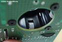
2.Two rollers inside the mouse touch the ball. One of the rollers is oriented so that it detects motion in the X direction, and the other is oriented 90 degrees to the first roller so it detects motion in the Y direction. When the ball rotates, one or both of these rollers rotate as well. The following image shows the two white rollers on this mouse:


3. The rollers each connect to a shaft, and the shaft spins a disk with holes in it. When roller rolls, its shaft and disk spin. The following image shows the disk:

4. On either side of the disk there is an infrared LED and an infrared sensor. The holes in the disk break the beam of light coming from the LED so that the infrared sensor sees pulses of light.


The rate of the pulsing is directly related to the speed of the mouse and the distance it travels

5. An on-board processor chip reads the pulses from the infrared sensors and turns them into binary data that the computer can understand. The chip sends the binary data to the computer through the mouse's cord.

In this optomechanical arrangement, the disk moves mechanically, and an optical system counts pulses of light. On this mouse, the ball is 21 mm in diameter. The roller is 7 mm in diameter. The encoding disk has 36 holes. So if the mouse moves 25.4 mm (1 inch), the encoder chip detects 41 pulses of light.
Each encoder disk has two infrared LEDs and two infrared sensors, one on each side of the disk (so there are four LED/sensor pairs inside a mouse). This arrangement allows the processor to detect the disk's direction of rotation. There is a piece of plastic with a small, precisely located hole that sits between the encoder disk and each infrared sensor. This piece of plastic provides a window through which the infrared sensor can "see." The window on one side of the disk is located slightly higher than it is on the other -- one-half the height of one of the holes in the encoder disk, to be exact. That difference causes the two infrared sensors to see pulses of light at slightly different times. There are times when one of the sensors will see a pulse of light when the other does not, and vice versa

ASSYMETRIC DIGITAL SUBSCRIBER LINE

ASSYMETRIC DIGITAL SUBSCRIBER LINE

Digital Subscriber Lines (DSL) are used to deliver high-rate digital data over existing ordinary phone-lines. A new modulation technology called Discrete Multitone (DMT) allows the transmission of high speed data. DSL facilitates the simultaneous use of normal telephone services, ISDN, and high speed data transmission, e.g., video. DMT-based DSL can be seen as the transition from existing copper-lines to the future fiber-cables. This makes DSL economically interesting for the local telephone companies. They can offer customers high speed data services even before switching to fiber-optics.


DSL is a newly standardized transmission technology facilitating simultaneous use of normal telephone services, data transmission of 6 M bit/s in the downstream and Basic- rate Access (BRA). DSL can be seen as a FDM system in which the available bandwidth of a single copper-loop is divided into three parts. The base band occupied by POTS is split from the data channels by using a method which guarantees POTS services in the case of ADSL-system failure (e.g. passive filters).

INTRODUCTION
The past decade has seen extensive growth of the telecommunications industry, with the increased popularity of the Internet and other data communication services. While offering the world many more services than were previously available, they are limited by the fact that they are being used on technology that was not designed for that purpose.

The majority of Internet users access their service via modems connects to the Plain Old Telephone System (POTS). In the early stages of the technology, modems were extremely slow by today’s standards, but this was not a major issue. A POTS connection provided an adequate medium for the relatively small amounts of data that required transmission, and so was the existing system was the logical choice over special cabling.

Technological advances have seen these rates increase up to a point where the average Internet user can now download at rates approaching 50Kbps, and send at 33.6Kps. However, POTS was designed for voice transmission, at frequencies below 3kHz, and this severely limits the obtainable data rates of the system. To increase performance of new online services, such as steaming audio and video, and improve general access speed, the bandwidth hungry public must therefore consider other alternatives. Technologies, such as ISDN or cable connections, have been in development for sometime but require special cabling. This makes them expensive to set up, and therefore have not been a viable alternative for most people.

DIFFERENT VARIANTS OF DSL .

HDSL- is the pioneering high speed format, but is not a commercially viable option due to its need for two twisted pairs and does not have support for normal telephone services.
SDSL- is symmetric DSL, and operates over a single twisted pair with support for standard voice transmission. The problem with this system is that it is limited to relatively short distances and suffers NEXT limitation due to the use of the same frequencies for transmitting and receiving.
IDSL- stands for ISDN DSL, and is in many ways similar to ISDN technology. It’s disadvantages are the lack of support for analog voice, and that its 128kbps rate is not much greater than that offered by standard 56kbps V90 modems.

VDSL- provides very high bit rate DSL, up to 52Mbps, but requires shorter connections lengths than are generally practical. It has been used in conjunction with an experimental project, FTTC (Fiber to the Curb), but development in this area has slowed due to commercial viability issues.

ADSL- is the most promising DSL technology, proving suitable for personal broadband requirements and allowing for the same channel to still act as a traditional POTS service.
Rate Adaptive DSL, RADSL-, is a further advancement which is able to automatically optimize the ADSL data rate to suit the conditions of the line being used.

BY-WIRE-STEERED SYSTEM

BY-WIRE-STEERED SYSTEM

By-wire-steered system is integration of electronic devices and mechanical systems in order to improve the performance of the steering system.Recent advances in dependable embedded system technology, as well as continuing demand for improved handling and passive and active safety improvements, have led vehicle manufacturers and suppliers to actively pursue development programs in computer-controlled, by-wire subsystems. These subsystems include steer and brake-by-wire, and are composed of mechanically decoupled sets of actuators and controllers connected through multiplexed, in-vehicle computer networks.A steer-by-wire system replaces the traditional mechanical linkage between the steering wheel and the road wheel actuator (e.g., a rack and pinion steering system) with an electronic connection. This allows flexibility in the packaging and modularity of the design. Since it removes the direct Kinematic relationship between the steering and road wheels, it enables control algorithms to help enhance driver input.There is no mechanical link to the driver.

Steer- and brake-by-wire provide a number of packaging and assembly advantages over conventional subsystems. For instance, electromechanical brake-by-wire subsystems require no hydraulic fluid to store or load at the assembly plant and permit more modular assembly, thus reducing the number of parts to be handled during production. Steer-by-wire systems have no steering column and may also eliminate cross-car steering assemblies such as racks. Arguments for ‘by-Wire’ systems include production costs, packaging and traffic safety . The ‘by-Wire’ technology as in drive, brake and steer is gaining ground and is undoubtedly an automotive solution of the future.

The arguments to support such ‘by-Wire’ systems include reduced production costs and packaging advantages and improved traffic safety. Emerging drive-by- wire technologies offer new possibilities for designing the steering characteristics of road vehicles. When the mechanical link between the steering wheel and the front wheels is replaced by sensors, controllers and actuators, enormous flexibility is achieved in terms of the control device applied and in terms of the transfer function of the steering system. This offers new possibilities for optimizing the steering system for mass-produced vehicles. However, the flexibility is of even greater advantage in the area of car adjustment for drivers with physical disabilities.The transition to purely electrical steering systems will take place step by step via systems with mechanical or hydraulic backup. Development and production of the next generations of electrical steering systems up to purely electrical steering systems create high safety demands on components and systems. Reliable and safe electrical steering systems can be realized by using appropriate safety techniques for these new systems and their components combined with the know-how of safety relevant vehicle systems.

The main limitations of by-wire-steered system are the requirement of a 42 Volts car supply, high output alternator and new generation batteries.The steer-by-wire principle becomes absolutely necessary when Future innovative steering functions, such as vehicle dynamic interventions, collision avoidance, individual wheel steering, tracking assistance, automatic lateral guidance, and finally autonomous driving functions have to be implemented in a system compound of various vehicle systems.

INTRODUCTION

By-wire-steered system is an application of ‘MECHATRONICS’, which is the integration of electronic devices and mechanical systems in order to improve the performance of the system .Recent advances in dependable embedded system technology, as well as continuing demand for improved handling and passive and active safety improvements, have led vehicle manufacturers and suppliers to actively pursue development programs in computer-controlled, by-wire subsystems. These subsystems include steer and brake-by-wire, and are composed of mechanically decoupled sets of actuators and controllers connected through multiplexed, in-vehicle computer networks. There is no mechanical link to the driver.

Steer- and brake-by-wire provide a number of packaging and assembly advantages over conventional subsystems. For instance, electromechanical brake-by-wire subsystems require no hydraulic fluid to store or load at the assembly plant and permit more modular assembly, thus reducing the number of parts to be handled during production. Steer-by-wire systems have no steering column and may also eliminate cross-car steering assemblies such as racks. Arguments for ‘by-Wire’ systems include production costs, packaging and traffic safety.The ‘by-Wire’ technology as in drive, brake and steer is gaining ground and is undoubtedly an automotive solution of the future.

The arguments to support such ‘by-Wire’ systems include reduced production costs and packaging advantages and improved traffic safety (a boon for everybody involved). Emerging drive-by- wire technologies offer new possibilities for designing the steering characteristics of road vehicles. When the mechanical link between the steering wheel and the front wheels is replaced by sensors, controllers and actuators, enormous flexibility is achieved in terms of the control device applied and in terms of the transfer function of the steering system. This offers new possibilities for optimizing the steering system for mass-produced vehicles. However, the flexibility is of even greater advantage in the area of car adjustment for drivers with physical disabilities.

A steer-by-wire system replaces the traditional mechanical linkage between the steering wheel and the road wheel actuator (e.g., a rack and pinion steering system) with an electronic connection. This allows flexibility in the packaging and modularity of the design. Since it removes the directKinematic relationship between the steering and road wheels, it enables control algorithms to help enhance driver input.The transition to purely electrical steering systems will take place step by step via systems with mechanical or hydraulic backup. Development and production of the next generations of electrical steering systems up to purely electrical steering systems create high safety demands on components and systems.

Reliable and safe electrical steering systems can be realized by using appropriate safety techniques for these new systems and their components combined with the know-how of safety relevant vehicle systems.‘Steer-by-Wire’ (SbW) there exists a legislation obstacle as European regulations require a mechanical connection between the steering wheel and the wheels. The column electric power steering (C-EPS) in the Opel Astra is therefore only an electric

hybridization at steering level: the steering torque levels will increase when the car picks up speed. The “Dual drive” system in the Fiat Punto has an EPS with dual settings: the driver can activate the “city” mode and obtain gentler steering when parking. The main limitations of by-wire-steered system are the requirement of a 42 Volts car supply, high output alternator and new generation batteries.The steer-by-wire principle becomes absolutely necessary when Future innovative steering functions, such as vehicle dynamic interventions, collision avoidance, individual wheel steering, tracking assistance, automatic lateral guidance, and finally autonomous driving functions have to be implemented in a system compound of various vehicle systems

PRO LOGIC II

Pro Logic II,
The next generation of Dolby Surround Pro Logic decoding technology. Pro Logic II brings exciting new features and advanced performance for decoding the many thousands of existing Dolby Surround programs, making them sound more like a discrete Dolby Digital 5.1-channel version than ever before.


The world is rapidly transitioning to digital delivery formats like DVD, and digital television (DTV), satellite and cable, all of which offer Dolby Digital 5.1 audio capability. The music industry is on the verge of transitioning from stereo to 5.1-channel sound with the new DVD-Audio format. Consumers enthusiastically demand 5.1-channel sound in new programs of all kinds. But vast numbers of programs already exist in stereo and Dolby Surround, and many more will continue to arrive in years to come. Pro Logic ­II lets consumers enjoy these programs with a convincing io5.1-likelc presentation.
Pro Logic II is able to decode the thousands of existing Dolby Surround movies and TV shows already on the shelf, compatibly, and with enhanced image stability. The improvements in decoding techniques mean that the discreteness of the sound field elements are better-preserved in the decoding process than was possible with the now universally standard Pro Logic technology, developed in the mid 80s.

“The technology in Pro Logic II is the first fundamentally new approach in matrix decoder design since the basic design which is still at the core of every other active matrix surround decoder” said Roger Dressler, Director of Technology Strategy for Dolby Laboratories.
“Pro Logic II was designed from the outset to convert conventional stereo music recordings, which will be with us for some time to come, to a natural, believable surround experience. The result is a decoder that can handle a wide range of movie and music program material with equal skill.
Dolby is proud to be handling the licensing and technical support of this exciting new technology”This new system was invented by Jim Fosgate, one of the most prolific developers of surround decoding technologies since the quadraphonic era of the late 1960s. Mr. Fosgate said,” I have spent the past 25 years figuring out how to expose the hidden information in standard two-channel stereo recordings, both new and old. This breakthrough in matrix decoding technology allows users to enjoy all their existing two-channel programs, whether Dolby Surround encoded or not, with an enhanced level of spatiality and directionality.”
Pro Logic II also incorporates special features for controlling the overall spatial dimensionality and frontal sound field imaging that are particularly suited for auto sound applications. A standard four-channel Pro Logic decoding mode is also included in the technology package.Dolby Surround Pro Logic II decoding can be implemented economically in either analog or digital circuitry, making it ideal for use in all traditional home theater products and in a range of new “music surround” products.

RFID for Automatic Authentication in Banks

RFID for Automatic Authentication in Banks

Abstract of this Seminar Topic.

RFID can be used to provide an easy and efficient way to authenticate people working in an organization. Authentication is necessary to restrict access to data stored in computers. Information stored in a bank’s database contains crucial data about consumers and the bank’s functioning. These data need to be kept securely. Unauthorized access to such information can’t be allowed. As a consequence authentication of personnel having access to such information is necessary.

Presently passwords are used for authentication. In case a person leaves after she has logged in using a password, any unscrupulous person can get access to the data and be in a position to change it. In situations where the passwords have been forgotten or have been changed the access to data is denied causing disruption in work. This can be detrimental to the running of the bank. Since authentication using passwords involves limitations related to human behavior there is a need for a better method for the same. Here is where RFID comes into play.

Radio frequency identification (RFID) is a method of remotely storing and retrieving data using devices called RFID tags. An RFID tag is a small object, such as an adhesive sticker, that can be attached to or incorporated into a product. RFID tags contain antennae to enable them to receive and respond to radio-frequency queries from an RFID transceiver. In the proposed system authentication of workers will be done with the help of RFID tag provided to them, which will uniquely identify them and give access to information meant only for them.

This is an economical alternative to the present system, which will have additional features like
Ø performance monitoring
Ø automatic attendance system
Ø providing mobility of data
Ø improved ATM service.


There is a centralized database having all the information. Readers will be positioned at appropriate places. Only with the tag can a person get access to her domain of information. There will be different levels of privileges for different people ranging from the customer to the manager of the bank.

Wednesday, August 12, 2009

Biochip

Biochip

The development of biochips is a major thrust of the rapidly growing biotechnology industry, which encompasses a very diverse range of research efforts including genomics, proteomics, and pharmaceuticals, among other activities. Advances in these areas are giving scientists new methods for unraveling the complex biochemical processes occurring inside cells, with the larger goal of understanding and treating human diseases. At the same time, the semiconductor industry has been steadily perfecting the science of microminiaturization. The merging of these two fields in recent years has enabled biotechnologists to begin packing their traditionally bulky sensing tools into smaller and smaller spaces, onto so-called biochips. These chips are essentially miniaturized laboratories that can perform hundreds or thousands of simultaneous biochemical reactions. Biochips enable researchers to quickly screen large numbers of biological analytes for a variety of purposes, from disease diagnosis to detection of bioterrorism agents.

A biochip is a collection of miniaturized test sites (microarrays) arranged on a solid substrate that permits many tests to be performed at the same time in order to achieve higher output and speed. Biochips can also be used to perform techniques such as electrophoresis or PCR using microfluidics technology (Fan, 2009; Cady, 2009).

== History ==oxygen electrode, thereby relating oxygen levels to glucose concentration. This and similar biosensors became known as enzyme electrodes, and are still in use today.

In 1953, Watson and Crick announced their discovery of the now familiar double helix structure of DNA molecules and set the stage for genetics research that continues to the present day (Nelson, 2000). The development of sequencing techniques in 1977 by Gilbert (Maxam, 1977) and Sanger (Sanger, 1977) (working separately) enabled researchers to directly read the genetic codes that provide instructions for protein synthesis. This research showed how hybridization of complementary single oligonucleotide strands could be used as a basis for DNA sensing. Two additional developments enabled the technology used in modern DNA-based biosensors. First, in 1983 Kary Mullis invented the polymerase chain reaction (PCR) technique (Nelson, 2000), a method for amplifying DNA concentrations. This discovery made possible the detection of extremely small quantities of DNA in samples. Second, in 1986 Hood and coworkers devised a method to label DNA molecules with fluorescent tags instead of radiolabels (Smith, 1986), thus enabling hybridization experiments to be observed optically.

Tuesday, August 11, 2009

Asynchronous circuit

Asynchronous circuit
An asynchronous circuit is a circuit in which the parts are largely autonomous. They are not governed by a clock circuit or global clock signal, but instead need only wait for the signals that indicate completion of instructions and operations. These signals are specified by simple data transfer protocols. This digital logic design is contrasted with a synchronous circuit which operates according to clock timing signals.
Theoretical foundations
Petri Nets are an attractive and powerful model for reasoning about asynchronous circuits. However Petri nets have been criticized by Carl Hewitt for their lack of physical realism (see Petri net#Subsequent models of concurrency). Subsequent to Petri nets other models of concurrency have been developed that can model asynchronous circuits including the Actor model and process calculi.
The term asynchronous logic is used to describe a variety of design styles, which use different assumptions about circuit properties. These vary from the bundled delay model - which uses 'conventional' data processing elements with completion indicated by a locally generated delay model - to delay-insensitive design - where arbitrary delays through circuit elements can be accommodated. The latter style tends to yield circuits which are larger and slower than synchronous (or bundled data) implementations, but which are insensitive to layout and parametric variations and are thus "correct by design."
Benefits
Different classes of asynchronous circuitry offer different advantages. Below is a list of the advantages offered by Quasi Delay Insensitive Circuits, generally agreed to be the most "pure" form of asynchronous logic that retains computational universality. Less pure forms of asynchronous circuitry offer better performance at the cost of compromising one or more of these advantages:
* Robust handling of metastability of arbiters.* Early Completion of a circuit when it is known that the inputs which have not yet arrived are irrelevant.* Possibly lower power consumption because no transistor ever transitions unless it is performing useful computation (clock gating in synchronous designs is an imperfect approximation of this ideal). Also, clock drivers can be removed which can significantly reduce power consumption. However, when using certain encodings, asynchronous circuits may require more area, which can result in increased power consumption if the underlying process has poor leakage properties (for example, deep submicrometer processes used prior to the introduction of high-K dielectrics).* Freedom from the ever-worsening difficulties of distributing a high-fanout, timing-sensitive clock signal.* Better modularity and composability.* Far fewer assumptions about the manufacturing process are required (most assumptions are timing assumptions).* Circuit speed is adapted on the fly to changing temperature and voltage conditions rather than being locked at the speed mandated by worst-case assumptions.* Immunity to transistor-to-transistor variability in the manufacturing process, which is one of the most serious problems facing the semiconductor industry as dies shrink.* Less severe electromagnetic interference. Synchronous circuits create a great deal of EMI in the frequency band at (or very near) their clock frequency and its harmonics; asynchronous circuits generate EMI patterns which are much more evenly spread across the spectrum.* In asynchronous circuits, local signaling eliminates the need for global synchronization which exploits some potential advantages in comparison with synchronous ones. They have shown potential specifications in low power consumption, design reuse, improved noise immunity and electromagnetic compatibility. Asynchronous circuits are more tolerant to process variations and external voltage fluctuations.
Disadvantages
* Increased Complexity* More Difficult to Design* the performance analysis of asynchronous circuits is a complicated problem
Applications
Asynchronous CPU
Asynchronous CPUs are one of several ideas for radically changing CPU design.
Unlike a conventional processor, a clockless processor (asynchronous CPU) has no central clock to coordinate the progress of data through the pipeline. Instead, stages of the CPU are coordinated using logic devices called "pipeline controls" or "FIFO sequencers." Basically, the pipeline controller clocks the next stage of logic when the existing stage is complete. In this way, a central clock is unnecessary. It may actually be even easier to implement high performance devices in asynchronous, as opposed to clocked, logic:
* components can run at different speeds on an asynchronous CPU; all major components of a clocked CPU must remain synchronized with the central clock;* a traditional CPU cannot "go faster" than the expected worst-case performance of the slowest stage/instruction/component. When an asynchronous CPU completes an operation more quickly than anticipated, the next stage can immediately begin processing the results, rather than waiting for synchronization with a central clock. An operation might finish faster than normal because of attributes of the data being processed (e.g., multiplication can be very fast when multiplying by 0 or 1, even when running code produced by a naive compiler), or because of the presence of a higher voltage or bus speed setting, or a lower ambient temperature, than 'normal' or expected.
Asynchronous logic proponents believe these capabilities would have these benefits:
* lower power dissipation for a given performance level, and* highest possible execution speeds.
The biggest disadvantage of the clockless CPU is that most CPU design tools assume a clocked CPU (i.e., a synchronous circuit). Many tools "enforce synchronous design practices". Making a clockless CPU (designing an asynchronous circuit) involves modifying the design tools to handle clockless logic and doing extra testing to ensure the design avoids metastable problems. The group that designed the aforementioned AMULET, for example, developed a tool called LARD to cope with the complex design of AMULET3.
Despite the difficulty of doing so, numerous asynchronous CPUs have been built, including:
* the ORDVAC (?) and the (identical) ILLIAC I (1951), * the ILLIAC II (1962);* The Caltech Asynchronous Microprocessor, the world-first asynchronous microprocessor (1988);* the ARM-implementing AMULET (1993 and 2000);* the asynchronous implementation of MIPS R3000, dubbed MiniMIPS (1998);* the SEAforth multi-core processor (2008) from Charles H. Moore.
The ILLIAC II was the first completely asynchronous, speed independent processor design ever built; it was the most powerful computing machine known to man at the time.
DEC PDP-16 Register Transfer Modules (ca. 1973) allowed the experimenter to construct asynchronous, 16-bit processing elements. Delays for each module were fixed and based on the module's worst-case timing.
The Caltech Asynchronous Microprocessor (1988) was the first asynchronous microprocessor (1988). Caltech designed and manufactured the world's first fully Quasi Delay Insensitive processor. During demonstrations, the researchers amazed viewers by loading a simple program which ran in a tight loop, pulsing one of the output lines after each instruction. This output line was connected to an oscilloscope. When a cup of hot coffee was placed on the chip, the pulse rate (the effective "clock rate") naturally slowed down to adapt to the worsening performance of the heated transistors. When liquid nitrogen was poured on the chip, the instruction rate shot up with no additional intervention. Additionally, at lower temperatures, the voltage supplied to the chip could be safely increased, which also improved the instruction rate -- again, with no additional configuration.

Adaptive cruise control System

Adaptive cruise control System

An automotive cruise control system that automatically slows down the car if it is moving too close to the vehicle in front of it. A radar or laser unit located behind the grille determines the speed and distance of the vehicle in front. When the distance is computed to be safe again, the system accelerates the car back to its last speed setting. Also called "active cruise control" and "intelligent cruise control.
Autonomous cruise control is an optional cruise control system appearing on some more upscale vehicles. The system goes under many different trade names according to the manufacture. These systems use either a radar or laser setup allowing the vehicle to slow when approaching another vehicle and accelerate again to the preset speed when traffic allows. ACC technology is widely regarded as a key component of any future generations of smart cars.
Types
Laser-based systems are significantly lower in cost than radar-based systems; however, laser-based ACC systems do not detect and track vehicles well in adverse weather conditions nor do they track extremely dirty (non-reflective) vehicles very well. Laser-based sensors must be exposed, the sensor (a fairly-large black box) is typically found in the lower grille offset to one side of the vehicle.
Radar-based sensors can be hidden behind plastic fascias; however, the fascias may look different from a vehicle without the feature. For example, Mercedes packages the radar behind the upper grille in the center; however, the Mercedes grille on such applications contains a solid plastic panel in front of the radar with painted slats to simulate the slats on the rest of the grille.
Radar-based systems are available on many luxury cars as an option for approx. 1000-3000 USD/euro. Laser-based systems are available on some near luxury and luxury cars as an option for approx. 400-600 USD/euro.
Cooperating systems
Radar-based ACC often feature a Precrash system, which warns the driver and/or provides brake support if there is a high risk of a collision. Also in certain cars it is incorporated with a lane maintaining system which provides power steering assist to reduce steering input burden in corners when the cruise control system is activated.
Examples of vehicles with adaptive cruise control
2005 Acura RLAudi A4 (see a demonstration on YouTube), A5, A6, A8, Q7BMW 7 Series, 5 series, 6 series, 3 series (Active Cruise Control)2004 Cadillac DTS, STS, XLR2007 Chrysler 300C2006 Ford Mondeo, Taurus, S-Max, Galaxy2003 Honda Inspire Accord, LegendHyundai Genesis (Smart Cruise Control, delayed)Infiniti M, Q45,QX56, G35, FX35/45/50 and G371999 Jaguar XK-R, S-Type, XJ, XF2000 Lexus LS430/460 (laser and radar), RX (laser and radar), GS, IS, ES 350, and LX 570Lincoln MKS, MKT1998 Nissan Cima, Nissan Primera T-Spec Models (Intelligent Cruise Control)1998 Mercedes-Benz S-Class, E-Class, CLS-Class, SL-Class, CL-Class, M-Class, GL-Class, CLK-Class (Distronic, removed in 2009 from certain US models)Range Rover SportRenault Vel SatisSubaru Legacy & Outback Japan-spec called SI-Cruise1997 Toyota Celsior, Sienna (XLE Limited Edition), Avalon, Sequoia (Platinum Edition), Prius, AvensisVolkswagen Passat, Phaeton, Touareg, 2009 GolfVolvo S80, V70, XC70, XC60

ACTUATOR ( AS-i)

ACTUATOR ( AS-i)
In recent years, automation technology has migrated to new methods of transferring information. Increasingly, field-level devices such as sensors and actuators have internal intelligence capabilities and higher communication demands. The AS-i bus system provides the solution for a digital serial interface with a single unshielded two-wire cable which replaces traditional cable harness parallel wiring between masters and slaves.
AS-i technology is compatible with any fieldbus or device network. Low-cost gateways exist to use AS-i with CAN, PROFIBUS, Interbus, FIP, LON, RS-485 and RS-232.
The AS-i uses the Isolation Penetration Technology. The AS-i follows the ISO/OSI model to successfully implement the master/slave communication.

64-Point FT Chip

64-Point FT Chip
A fixed-point 16-bit word-length 64-point FFT/IFFT processor developed primarily for the application in an OFDM based IEEE 802.11a wireless LAN base band processor. The 64-point FFT is realized by decomposing it in to a two dimensional structure of 8-point FFTs. This approach reduces the number of required complex multiplication compared to the conventional radix-2 64-point FFT algorithm. The complex multiplication operations are realized using shift and add operation. Thus, the processor does not use a two-input digital multiplier. It also does not need any RAM or ROM for internal storage of coefficients. The core area of this chip is 6.8mm². The average dynamic power consumption is 41mW at 20Mhz operating frequency and 1.8Volt supply voltage. The processor completes one parallel-to-parallel 64-point FFT computation in 23 cycles; it can be used for any application that requires fast operation as well as low power consumption.

Three-dimensional integrated circuit(3-D ICs)

Three-dimensional integrated circuit(3-D ICs)
In electronics, a three-dimensional integrated circuit (3D IC, 3D-IC, or 3-D IC) is a chip with two or more layers of active electronic components, integrated both vertically and horizontally into a single circuit. The semiconductor industry is hotly pursuing this promising technology in many different forms, but it is not yet widely used; consequently, the definition is still somewhat fluid.
3D ICs vs. 3D packaging
3D packaging saves space by stacking separate chips in a single package. This packaging, known as System in Package (SiP) or Chip Stack MCM, does not integrate the chips into a single circuit. The chips in the package communicate with off-chip signaling, much as if they were mounted in separate packages on a normal circuit board. In contrast, a 3D IC is a single chip. All components on the layers communicate with on-chip signaling, whether vertically or horizontally. Essentially, a 3D IC bears the same relation to a 3D package that an SoC bears to a circuit board.

Manufacturing technologies
As of 2008 there are four ways to build a 3D IC:
Monolithic – Electronic components and their connections (wiring) are built in layers on a single semiconductor wafer, which is then diced into 3D ICs. There is only one substrate, hence no need for aligning, thinning, bonding, or through-silicon vias. Applications of this method are currently limited because creating normal transistors requires enough heat to destroy any existing wiring.
Wafer-on-Wafer – Electronic components are built on two or more semiconductor wafers, which are then aligned, bonded, and diced into 3D ICs. Each wafer may be thinned before or after bonding. Vertical connections are either built into the wafers before bonding or else created in the stack after bonding. These “through-silicon vias” (TSVs) pass through the silicon substrate(s) between active layers and/or between an active layer and an external bond pad.
Die-on-Wafer – Electronic components are built on two semiconductor wafers. One wafer is diced; the singulated dies are aligned and bonded onto die sites of the second wafer. As in the wafer-on-wafer method, thinning and TSV creation are performed either before or after bonding. Additional dies may be added to the stacks before dicing.
Die-on-Die – Electronic components are built on multiple dies, which are then aligned and bonded. Thinning and TSV creation may be done before or after bonding.
Benefits
3D ICs offer many significant benefits, including:
Footprint – More functionality fits into a small space. This extends Moore’s Law and enables a new generation of tiny but powerful devices.
Speed – The average wire length becomes much shorter. Because propagation delay is proportional to the square of the wire length, overall performance increases.
Power – Keeping a signal on-chip reduces its power consumption by ten to a hundred times. Shorter wires also reduce power consumption by producing less parasitic capacitance. Reducing the power budget leads to less heat generation, extended battery life, and lower cost of operation.
Design – The vertical dimension adds a higher order of connectivity and opens a world of new design possibilities.
Heterogeneous integration – Circuit layers can be built with different processes, or even on different types of wafers. This means that components can be optimized to a much greater degree than if they were built together on a single wafer. Even more interesting, components with completely incompatible manufacturing could be combined in a single device.
Circuit security - The stacked structure hinders attempts to reverse engineer the circuitry. Sensitive circuits may also be divided among the layers in such a way as to obscure the function of each layer.
Bandwidth - 3D integration allows large numbers of vertical vias between the layers. This allows construction of wide bandwidth buses between functional blocks in different layers. A typical example would be a processor+memory 3D stack, with the cache memory stacked on top of the processor. This arrangement allows a bus much wider than the typical 128 or 256 bits between the cache and processor. Wide buses in turn alleviate the memory wall problem.